The Frustrated Pairs Revolution
How Chemical Frustration is Enabling Cooler, Greener Electronics
The Semiconductor Dilemma: A Problem of Heat
Imagine trying to write with an ink that only works if your paper is glowing red hot. This is precisely the challenge material scientists have faced for decades in manufacturing semiconductors—the building blocks of all modern electronics. Conventional methods for depositing crucial elements like silicon and germanium onto surfaces require extreme temperatures, often exceeding 800-1000°C.
This high-temperature requirement has limited the materials we can use, driven up energy costs, and created significant manufacturing bottlenecks. But what if we could teach these elements to settle comfortably onto surfaces at a fraction of the heat?
Recent breakthroughs in a fascinating area of chemistry known as frustrated Lewis pairs (FLPs) are turning this possibility into reality, potentially revolutionizing how we build our electronic world while making the process remarkably cooler.


The Chemistry of Frustration: When Acids and Bases Can't Stand Each Other
To understand the magic behind this breakthrough, we need to revisit some basic chemistry concepts: Lewis acids and Lewis bases. Simply put, a Lewis base is a molecule that donates a pair of electrons (imagine someone eager to share), while a Lewis acid accepts electrons (imagine someone eager to receive). Normally, when these two meet, they instantly form a stable bond called an adduct, neutralizing each other's reactivity.
The revolutionary concept of frustrated Lewis pairs (FLPs) changes this dynamic entirely. Imagine a Lewis acid and base brought together on a blind date, but both are wearing such bulky outfits that they can't get close enough to interact properly.
This steric hindrance creates "frustration"—neither can achieve the neutral adduct they would normally form. This frustration leaves both molecules in a perpetually reactive state, poised to interact with other molecules in their environment 2 5 .
This "frustrated" state becomes incredibly useful because these pairs can work together to activate other molecules. Most notably, certain FLPs can perform the remarkable feat of splitting hydrogen molecules (H₂) into positively charged protons (H⁺) and negatively charged hydrides (H⁻) without needing expensive precious metals 2 . This metal-free activation of hydrogen was a landmark discovery that opened up new possibilities in catalysis and materials science.
Table 1: Key Components of Frustrated Lewis Pairs
| Component | Role | Characteristic | Example in FLPs |
|---|---|---|---|
| Lewis Acid | Electron acceptor | Typically boron-containing compounds with steric bulk | B(C₆F₅)₃, BCy₂ (Cy = cyclohexyl) |
| Lewis Base | Electron donor | Often phosphorus or nitrogen-containing compounds with large substituents | PR₃ (where R = bulky organic groups) |
| The "Frustration" | Prevents adduct formation | Creates unquenched reactivity | Steric hindrance from large molecular groups |

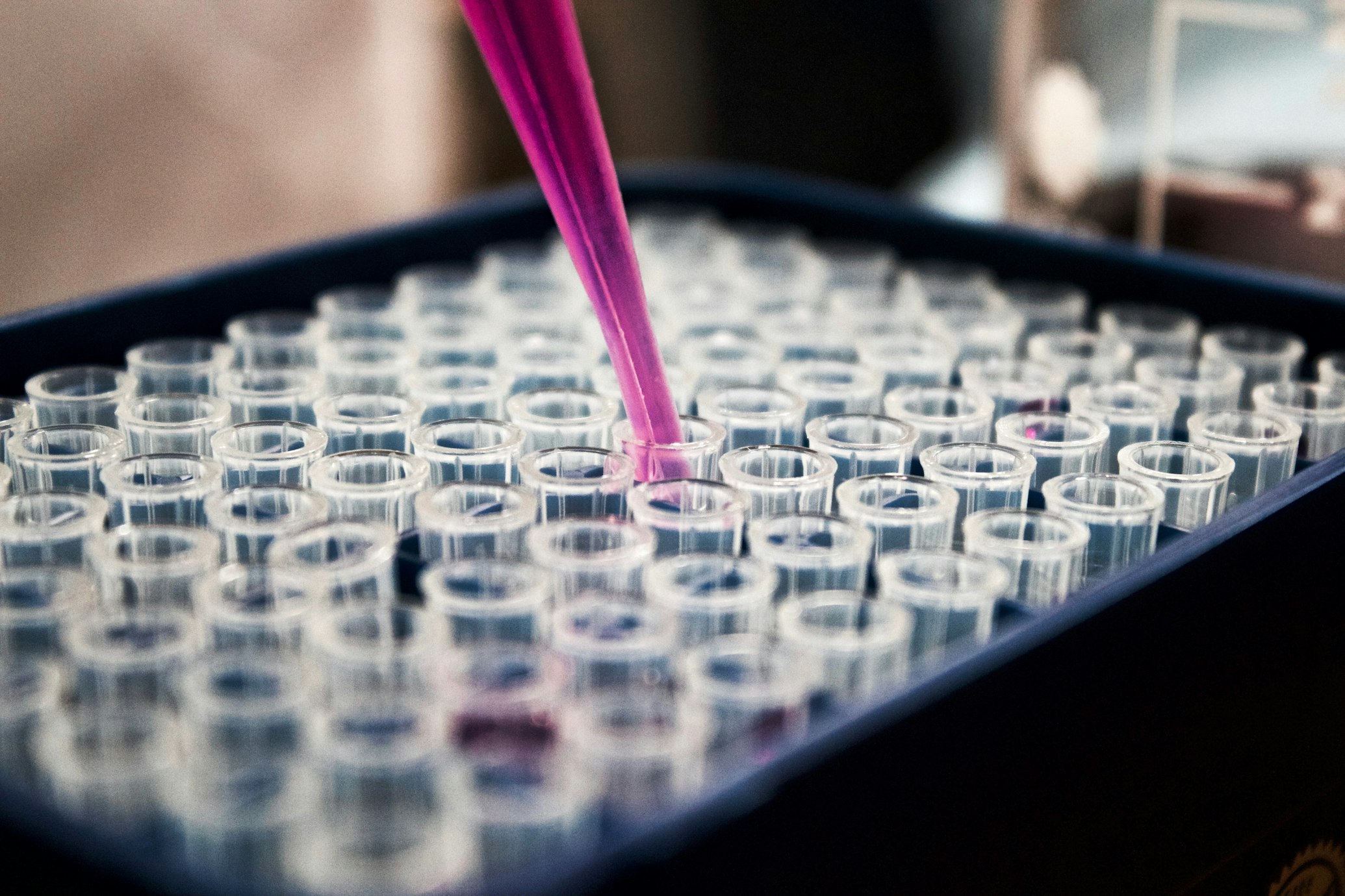
The Breakthrough Experiment: Low-Temperature Deposition in Action
In 2020, researchers achieved a remarkable advance by designing a specific FLP system to stabilize highly reactive silicon(II) and germanium(II) dihydrides—compounds that would typically decompose rapidly at room temperature. The key innovation was using an intramolecular FLP ligand called PB, iPr₂P(C₆H₄)BCy₂, where a phosphine (Lewis base) and borane (Lewis acid) are connected in the same molecular structure but sterically prevented from quenching each other's reactivity 1 .
Experimental Methodology: A Step-by-Step Process
Ligand Synthesis
Researchers first prepared the specialized FLP ligand (PB) where the phosphine and borane components were linked by a rigid molecular bridge, maintaining their separation and frustration 1 .
Stabilization of Reactive Intermediates
The PB ligand was then combined with silicon and germanium dihydride precursors. The FLP formed protective "chelates" around these highly reactive group 14 elements 1 .
Mild Thermolysis for Deposition
When gently heated in solution to a remarkably low 110°C, the stabilized compounds underwent controlled decomposition, releasing elemental silicon or germanium 1 .
Ligand Recovery
After deposition, the PB ligand could be recovered and recycled, creating an efficient "closed-loop" system that minimizes waste 1 .
Remarkable Results and Significance
The data from these experiments revealed extraordinary advances in materials deposition:
Table 2: Record-Low Deposition Temperatures Achieved via FLP Chelation
| Element Deposited | Traditional Deposition Temperature | FLP-Based Deposition Temperature |
|---|---|---|
| Silicon (Si) | 800-1000°C+ (conventional CVD) 4 | 110°C (from solution) 1 |
| Germanium (Ge) | Typically >600°C | Similarly low temperatures via FLP approach 1 |
| Tin (Sn) | Varies by method | Room temperature deposition demonstrated using related molecular approaches 7 |
The implications of these results are profound. The ability to deposit semiconductor elements at 110°C rather than near 1000°C represents a dramatic reduction in energy requirements. Additionally, the "closed-loop" system where the FLP ligand can be recycled after deposition marks significant progress toward more sustainable manufacturing processes 1 .
Beyond the Lab: Applications and Implications
The ramifications of low-temperature FLP-assisted deposition extend across multiple technological domains:
Transforming Semiconductor Manufacturing
Traditional chemical vapor deposition (CVD) processes dominate semiconductor manufacturing but carry significant limitations. The extremely high temperatures required can damage heat-sensitive components, limit substrate choices, and create substantial energy costs.
Flexible Electronics
Direct deposition of semiconductors onto plastic substrates that would melt at conventional processing temperatures.
Energy Efficiency
Dramatically lower deposition temperatures translate to reduced energy consumption and costs.
Sustainable Polymer Synthesis
Beyond elemental semiconductors, the FLP approach has demonstrated remarkable capability in polymer synthesis. The formation of poly(dimethylsilane) through controlled decomposition of [PB{SiMe₂}] suggests a pathway to various specialty polymers with tailored properties 1 . This method offers superior control over polymer structure compared to conventional approaches.
Environmental Benefits and Green Chemistry
Metal-Free Catalysis
Unlike many industrial processes that rely on expensive precious metals, FLP systems use abundant main-group elements .
Energy Efficiency
Dramatically lower deposition temperatures translate to reduced energy consumption.
Closed-Loop Systems
The recyclability of the FLP ligands minimizes waste generation 1 .
The Future of FLP Technology: Solid-State Applications and Beyond
As research progresses, scientists are already developing the next generation of FLP systems. A groundbreaking 2024 study published in Angewandte Chemie International Edition demonstrated the creation of solid-state FLPs using polymer-derived ceramics .
This innovation involves embedding FLP active sites within a sodium-doped amorphous silicon-boron-nitride (Na-doped SiBN) matrix, creating a material with exceptional thermal stability that can withstand temperatures up to 1000°C while maintaining catalytic activity .
These solid-state FLPs represent a crucial advancement for industrial applications, as they bridge the gap between the precise control of molecular FLPs and the rugged stability required for commercial processes.
Development of Chiral FLPs
For enantioselective synthesis of pharmaceuticals and specialty chemicals 3 .
Expansion to Broader Element Portfolios
Including compound semiconductors like indium phosphide, accessed through FLP-mediated phosphinidene transfer 7 .
Integration with Emerging Technologies
Hybrid ALD/CVD systems for atomic-scale precision in quantum computing components 8 .
Table 3: Essential Research Reagents in FLP Chemistry
| Research Reagent | Function | Specific Role |
|---|---|---|
| iPr₂P(C₆H₄)BCy₂ (PB Ligand) | Intramolecular FLP | Chelates and stabilizes reactive Si(II)/Ge(II) species |
| Tris(pentafluorophenyl)borane | Lewis acid component | Common in intermolecular FLPs for small molecule activation |
| Tricyclohexylphosphine (PCy₃) | Lewis base component | Sterically hindered base that resists adduct formation |
| Polysilazane Pre-ceramic Polymers | Support matrix | Forms amorphous silicon nitride for solid-state FLP systems |
Conclusion: A Cooler Path to a High-Tech Future
The development of frustrated Lewis pair chelation as a vehicle for low-temperature semiconductor and polymer deposition represents more than just a laboratory curiosity—it signals a fundamental shift in how we approach materials synthesis.
By harnessing molecular "frustration" rather than brute-force thermal energy, scientists have opened a pathway to more precise, efficient, and sustainable electronics manufacturing. As this technology matures and integrates with industrial processes, we may look back at these discoveries as the moment when our digital world learned to build itself without burning up.
The future of electronics isn't just smaller and faster—it's cooler, in every sense of the word.